In the past years I always had some DIY electronics related projects, which I tried to make somehow at home. For prototyping the breadboards are fine, but as soon as you have to make the next steps to create a stable and final hardware, you should work with PCBs. I do not count with pre-made prototype PCBs, which have their structured and distributed pads and traces across the board. These are not so good for SMD parts, moreover, the overall look with them will be most probably just simply disgusting not professional.
So, if you would like to work with your own designed and nice PCBs, then you can chose from several PCB manufacturers who support hobbyists with low cost and low quantity PCB production. However, for early prototyping there are some issues with them:
- You have to wait 1-2 weeks or even more before you get your boards, or you should pay much more for fast production/delivery.
- HW development is pretty much the same as SW development. In case of a complex project, there is a big chance to have some issues with your first (and second, and third…) board. So you have to pay for every variants and wait much more for the production/delivery.
If you make PCBs often, it is definitely worth to create your own “PCB fab” at home, to be able to prototype your own PCBs quickly. Then, if it is still necessary, you can order the final version from a professional manufacturer.
I am not a big fan of the toner transfer and other alternate methods and as I used to make projects in the school by photoresist PCBs, I decided to create an UV exposure “tool” for this purpose.
Plenty of DIY PCB UV exposure tool building posts are available on the internet with total different approaches. I also designed my own, to fulfill my needs: it should be relative small and portable and the hacking/modding should be fun. 🙂 Flat bed scanners were found as possibly good target. Compared to most of the other scanner mods, which use LED arrays or fluorescent tubes across the whole scanner bed area, my plan was to use the scanner carriage with only few LEDs and control its movement (and brightness) under the given PCB.
After a quick search on the local second hand portal I found a nice old Mustek 1200CP for about 4 EUR. I made the investment 🙂 and started the work.
The first task was to disassemble the scanner and to identify reusable parts.


The interesting components were:
- MITSUMI M35SP-7N bipolar stepper motor
- ULN2003A IC as a stepper driver (in fact this is a NPN Darlington array)
- 2 opto gate in special housing for the carriage return detection and for the scanner lid opening/closing detection
- DC connector 🙂
I wanted to keep the scanner housing, all mechanical parts and the interesting components listed above, then replace the controller board with a custom one. All dimensions of the original board were measured, since the custom controller was planned to the same place.
I quickly created a test setup to drive the stepper with a Pro Mini and ULN2003A. The core Arduino Stepper library was my first choice to do the job, but later I switched to AccelStepper library, which provided better controlling options.


The current limiting resistor become warm, even without any load on the stepper. After 1-2 minutes of simple running loop I measured 63 Celsius. This was the highest temperature, even in case of longer running cycles. Just to be on the safe side I planned to use a bigger power resistor on my board.
I had my plans with the controller board, but it was easier and faster to start with the LED panel. My previously ordered UV LED pack was used, 100 pieces cost 3.94$. Well, 0.74$ for shipping in advance. Still a cool deal, of course from China. These are wide angled LEDs, as the distance between the scanner’s carriage (where the LED board is) and the exposed PCB board is not too much. This way it is possible to avoid unexpected spots and the whole illumination could be smoothly distributed.


Not a complex circuit, right? As at this phase I did not have the hacked scanner ready, I had to fall back to the ugly toner transfer method. I hated it… for the 6th round I finally got a nice result when I removed the paper from the PCB, so it was time to finalize the board.


In the meantime I was working on the controller to drive the scanner. To be able to get the results as soon as possible the controller was quickly prototyped on a breadboard with Arduino Pro Mini. It worked, but during the development the code reached the MCU’s limits and I had to switch to Arduino Mega.


It was time to test the setup. A test PCB design was created, printed to tracing paper then multiple exposing rounds were executed on different boards with different settings.


The 4th the result looked pretty good, so after developing it I etched it. Traces and pads were nice and sharp, there was no issue with 6 mil traces as it is visible on the pictures captured from the USB microscope.


Ok, in fact there was one little issue at one of the TQFP32’s bottom middle pin, but due to the fact how the other parts looks like it was caused most probably by over-development or a photoresist material quality issue. Basically I was more than happy with the results, I thought that the calibration could be more time consuming.
This time I finalized the controller board design. It definitely needed more time than the LED panel 🙂
Main properties of the controller:
- ATmega2560 8-bit AVR microcontroller
- ICSP and serial (for FTDI) connectors exposed
- TLP124F single optocoupler with IRLZ34N MOSFET for the isolated UV LED PWM control on 12V
- RGB LED for visual feedback on different statuses (it is visible through the scanner’s closed lid), a small buzzer for the sound based feedbacks (menu “ticking”, error alerts, job end signal etc.)
- ULN2003A Darlington array to drive the stepper
- 2 opto gates (saved from the original controller) to detect the carriage return and the scanner’s lid status
- 12V (6.5V-23V) to 5V DC-DC step down converter to power the 5V electronics
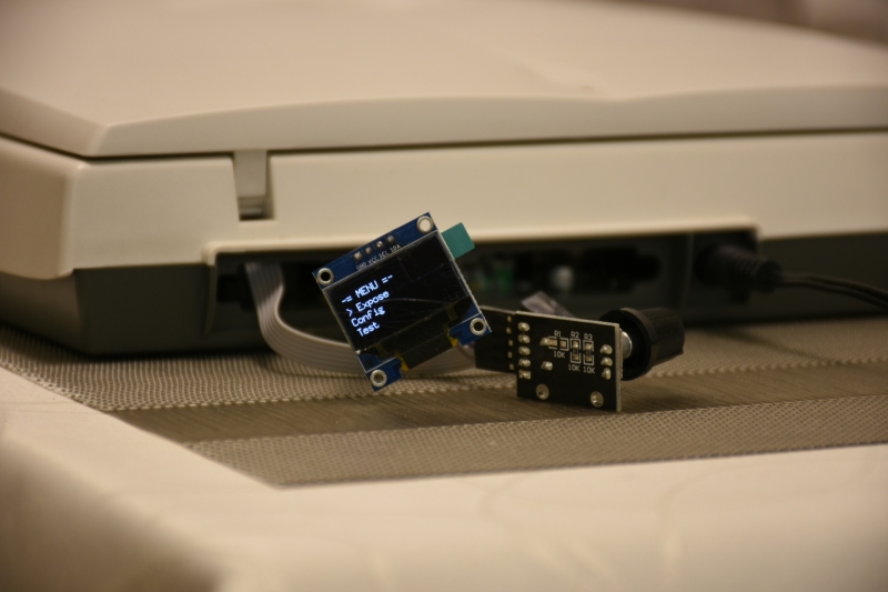
- 128×64 pixel 0.96″ I2C OLED panel with a rotary encoder for the menu and user input handling


As proper values for exposing were revealed, the next trivial step was to expose my custom controller board with the scanner. Unfortunately, as it was discovered later, my printer was the bottleneck in the process. It could print fine 6 mil traces, but with relative big clearing (about 10+ mil) only. Otherwise the printout contains unexpected paint spots between the traces, which of course have a big negative effect on the exposure itself. See the merged traces and TQFP100 pads on the picture below. Note that disappearing traces were caused by the over development and etching, while I tried to fix the unexpected connections.


To quickly overcome on the issue, the design was sent to a local PCB manufacturer for fabrication (so sad). As the PCB was supposed to be a demo version only, solder mask and silkscreen were not ordered. I would have been happy if I could make this board with the PCB UV exposure scanner itself, but at least, this way I was saved from the board outline cutting 🙂 which could be challenging at home for the given outline structure. I soldered all components, coded the firmware and tested the board. Fortunately everything worked as expected.


Currently the UV exposure scanner is reliable and works as expected, even with fine traces, but I have issues with the small clearings due to my printer’s capabilities. It is more than enough for a lot of my projects, however I will try to fix this issue later (maybe by replacing the printer) as some designs really need 6mil/6mil traces/clearance.
There are still some tasks to complete before the job is done. Just to mention some:
- Implementing the remaining functionalities to the firmware (e.g. better menu handling, improved auto carriage position calibration and homing).
- Code cleaning and releasing (in the meantime if anyone would like to replicate the project, here is the actual hex file).
- Mounting the display and the rotary encoder to the scanner’s front panel and connecting it to the controller board with a ribbon cable.
So, to be continued later…

Hi. Nice project. What was the feed speed for optimum exposure time? Do you know the wavelength of your LEDs? Thx.
LikeLike
thanks! the LEDs have 395nm – 400nm wavelength, just see the linked item page for the details. using tracing papers with laser printed mask my working config has the following settings: speed: 50, PWM: 80%, count: 5. PWM and count is quite self explanatory, but the speed is a bit tricky as it reflects to the stepper’s speed (steps per second). I think the real speed factor is not too interesting, as it will really vary on the implemented setup, e.g. on your LEDs , the current you are using to drive the LEDs, photoresist materials etc. this is the reason why I made it possible to create profiles in the controller, so you can store multiple working settings for different materials/jobs, but basically this should be experienced by the owner during the first rounds.
LikeLike
Hello Andrew, thanks for the info. I understand that it depends, but it would be great if you could say that for your setup you can do XX cm / min, so people can have a clue about how long it will take to exposure the PCB through tracing paper with power of 45 China’s LEDs in row @ 400 nm. Thanks.
LikeLiked by 1 person
Andrew? Please give us the approximate time per cm for exposure time. Thanks.
LikeLike
So, Awen, after the Christmas and new year celebration I finally managed to measure it. With my currently used profile (speed 50, count 5) it takes 3:52 to expose a 5cm wide PCB (it could be 5x22cm).
LikeLike
Thank you for the info. I have currently a quite powerful UV setup (5x 18W UV-A neon tubes) and it takes 60-75 seconds @ distance of 10 cm @ 365 nm to exposure the pcb. Optical power is around 5 watts. Yours 45 leds have optical power of around 0.3 watt. I want to try this setup with scanner bed but with more powerful UV leds with around 3 watts of optical power total. Hopefully I will be able get it under a minute per 10 cm.
LikeLike
Hi, nice job!
I’ve found an old scanner in my storage room and I was thinking about what could I do with It since I started to “play” with Arduino few weeks ago. Then I found your post….
I would like to try to do something similar.
You posted the hex code, but, I can’t deal with It…
Could you send me the Arduino code, pls?
Thx.
LikeLike
Hi Andrew, very nice job!
I’ve found an old scanner and I was thinking to replicate your project
You posted the hex code, but, I can’t read it. Could you send me the Arduino IDE code, pls? thanks Andrea
LikeLike
Hello Andrea,
I’m not actively maintaining the code and it is not ready to be shared.
The hex file is still there and works, if you flash it to your MCU.
Good luck for the developments!
LikeLike